Application note on quartz crystal oscillator
来源:http://www.taiheth.com 作者:泰河电子晶振 2019年07月24
The purpose of these application notes is to help customers in specifying Clock Oscillators. Background information about the type of Oscillators offered by ECS is included along with some common definitions and helpful formulas. The ECS Oscillator product line consists of Clock Oscillators, TCXOs,VCXOs, VCTCXOs and VCOs.
Clock Oscillator: The standard clock oscillator is the most common type of oscillator used and has applications in virtually every aspect of the electronics industry. The clock oscillator is used to establish a reference frequency used for timing purposes. A typical application is the sequencing of events in a computer.
A crystal controlled clock oscillator typically consists of an amplifier and a feedback network that selects a part of the amplifier output and returns it to the amplifier input. A simplified block diagram of such a circuit is shown below in (Fig 1).
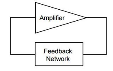
Figure 1) Simplified Block Diagram of a Crystal Controlled Clock Oscillator
The basic criteria for oscillation in an oscillator are: 1. The open loop gain must be greater than the losses around the oscillator loop and 2. The phase shift around the oscillator loop must be either 0 or 360 degrees.
An oscillator can be used to generate different types of waveforms. The most common types of waveforms produced by an oscillator are sinusoidal and square.
The Main parameters used in specifying a clock oscillator are listed below.
Logic TTL, HCMOS: In general, an HCMOS oscillator with drive TTL circuitry (not vice versa). The industry is moving away from the TTL logic as IC manufacturers are discontinuing the supply for many common TTL IC's. Most ECS clock oscillators are HCMOS/ TTL compatible.
Frequency Stability: The most common stabilities are 25, 50 and 100 PPM. Overall stability usually includes accuracy at 25°C, effects due to changes in operating temperature, input voltage, aging, shock and vibration. The ± 100PPM stability has been the most popular as it is sufficient to run microprocessors. The Telecommunications industry has been moving toward tighter and tighter stabilities. Stabilities beyond ± 100PPM are no longer offered in commercial (0-70°C) applications, since standard process controls achieve this stability as a minimum. Requesting 50 PPM is usually a little more expensive. Clock oscillators requiring 25 PPM can significantly affect the price. For tighter than 25 PPM stability applications, please consult the factory or consider a TCXO.
TCXOs (Temperature Compensated Crystal Oscillators)
Typically consist of tight tolerance quartz crystal, a temperature compensation network, an oscillator circuit and a variety of buffer and/or output stages determined by the output requirement. The crystal has a characteristic of changing frequency when a capacitor is inserted in series with the crystal unit as shown in (Fig. 2)
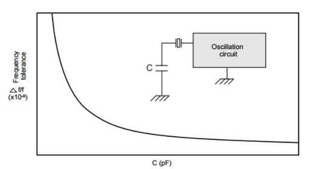
Figure 2) Load Capacitance Characteristics of Crystal Unit
Utilizing the above characteristics, frequency can be stabilized by inserting a temperature compensation circuit consisting of thermistors, resistors and capacitors in the oscillation look as shown in (Fig. 3). The temperature compensation network is used to sense the ambient temperature and “pull” the crystal frequency in a manner which reduces frequency vs. temperature effect of the quartz crystal.
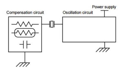
Figure 3) Temperature Compensation Circuit
A TCXO is generally required when overall stability needs are greater than those of a clock oscillator.Also, the long-term aging effects of a TCXO are better than those of most clock oscillators.
Input Voltage: Most TCXOs are designed to operate at 5VDC, 3.3 VDC or a combination of both.
RF Output: A TCXO can be manufactured with various types of outputs: sine wave, clipped sine wave,TTL, HCMOS and ECL. Be sure to specify the desired output type, signal requirements and the load that the oscillator will be driving.TCXOs also have a frequency adjustment feature which allow for readjustment of the oscillator to its center frequency to compensate for aging. This adjustment can be provided in the following ways.
1) A mechanical adjustment (internal trimmer) within the oscillator accessible via hole in the enclosure.
2) An electrical adjustment via a lead in the enclosure for either a remotely located potentiometer or a voltage. An oscillator using this technique is called a Temperature Compensated Voltage Controlled Crystal Oscillator or TCVCXO.
3) A combination of both mechanical and electrical adjustment.
VCXOs (Voltage Controlled Crystal Oscillator) are crystals controlled oscillators in which the output frequency can be adjusted by varying the external control voltage across a variable capacitor ( varactor diode) within the oscillator circuit. The associated change in frequency due to the change in control voltage is known as pullability. VCXOs are used widely in telecommunications, instrumentation and other electronic equipment where a stable but electrically tunable oscillator is required.
The varactor diode is a semiconductor device that is designed to act as a variable capacitor when a voltage is applied to it. When used in series with crystal , as shown in (Fig. 4), changing the control voltage causes diode capacitance to change. This change in capacitance causes the total crystal load capacitance to change and subsequently causes a change in crystal frequency.
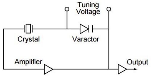
Figure 4) Typical VCXO Circuit
Due to the growing applications of VCXOs in digital data transmissions phase jitter (short-term stability) has become an important consideration. Phase jitter provides a precise way to establish when a phase transition occurs.
Definitions: The following definitions will aid you in understanding oscillator performance and terminology.
Nominal Frequency: The center or nominal output of a crystal oscillator.
Frequency Tolerance: The deviation from the nominal frequency in terms of parts per million (PPM) at room temperature. (25°C ± 5°C)
Frequency Range: The frequency band that the oscillator type or model can be offered.
Frequency Stability:The maximum allowable frequency deviation compared to the measured frequency at 25°C over the temperature window, ie 0°C to +70°C. The typical stability for clock oscillators is ±0.01% (±100PPM).
Operating Temperature: Temperature range within which output frequency and other electrical,environmental characteristics meet the specifications.
Aging: The relative frequency change over a certain period of time. Typically aging for clock oscillators is ±5PPM over 1 year maximum.
Storage Temperature: The temperature range within which the unit is safely stored without damaging or changing the performance of the unit.
Supply Voltage: The maximum voltage which can safely be applied to the VCC terminal with respect to ground.
Input Voltage (VIN): The maximum voltage which can be safely applied to any input terminal of the oscillator.
Output HIGH Voltage (VOH): The minimum voltage at an output of the oscillator under proper loading.
Output LOW Voltage (VIH): The maximum voltage to guarantee threshold trigger at the input of the oscillator.
Supply Current: The Current flowing into Vcc terminal with respect to ground. Typically supply current is measured without load.
Symmetry of Duty Cycle: The symmetry of the output waveform at the specified level (at 1.4 V for TTL, at 1/2 Vcc for HCMOS, or 1/2 waveform peak level for ECL).
Rise Time (TR): Waveform rise time from Low to High transition measured at the specified level (20% to 80% for HCMOS, ECL and 0.4 V to 2.4 V for TTL).
Fall Time (TF): The waveform fall time from High to Low transition, measured at the specified level (80% to 20% for the HCMOS, ECL and 2.4 V to 0.4 V for TTL).
Load/Fan Out: The maximum load that the different families of oscillators can drive is defined as the output load driving capability. The load driving capability (fan-out) of each family of oscillators is specified in terms of the number of gates an oscillator can drive.
Jitter (short-term stability): The modulation in phase or frequency of the oscillator output.
HCMOS/TTL Compatible: The oscillator is designed with ACMOS logic with driving capability of TTL and HCMOS loads while maintaining minimum logic High of HCMOS.
Tri-State Enable: When the input is left OPEN or tied to logic “1” the normal oscillation occurs. When the input is grounded (tied to logic “0”, the output is HIGH IMPEDANCE state. The input has an internal pull-up resistor thus allowing the input to be left open.
Output Logic: The output of an oscillator is designed to meet various specified logic's such as TTL,HCMOS, ECL, Sine, Clipped-Sine (DC cut).
Harmonic Distortion: The non-linear distortion due to unwanted harmonic spectrum component related with target signal frequency. Each harmonic component is the ratio of electric power against desired signal output electric power and is expressed in terms of dbc, ie -20 dBc. Harmonic distortion specification is important especially in sine output when a clean and less distorted signal is required.
Dual and Multiple Outputs: More than one signal is capable of being generated from a single oscillator.The signals may be related (usually a multiple or divisor of the signal produced by a single crystal).
Start-Up Time: The start up time of an oscillator is defined as the time an oscillator takes to reach its specified RF output amplitude.
Clock Oscillator: The standard clock oscillator is the most common type of oscillator used and has applications in virtually every aspect of the electronics industry. The clock oscillator is used to establish a reference frequency used for timing purposes. A typical application is the sequencing of events in a computer.
A crystal controlled clock oscillator typically consists of an amplifier and a feedback network that selects a part of the amplifier output and returns it to the amplifier input. A simplified block diagram of such a circuit is shown below in (Fig 1).
Figure 1) Simplified Block Diagram of a Crystal Controlled Clock Oscillator
The basic criteria for oscillation in an oscillator are: 1. The open loop gain must be greater than the losses around the oscillator loop and 2. The phase shift around the oscillator loop must be either 0 or 360 degrees.
An oscillator can be used to generate different types of waveforms. The most common types of waveforms produced by an oscillator are sinusoidal and square.
The Main parameters used in specifying a clock oscillator are listed below.
Logic TTL, HCMOS: In general, an HCMOS oscillator with drive TTL circuitry (not vice versa). The industry is moving away from the TTL logic as IC manufacturers are discontinuing the supply for many common TTL IC's. Most ECS clock oscillators are HCMOS/ TTL compatible.
Frequency Stability: The most common stabilities are 25, 50 and 100 PPM. Overall stability usually includes accuracy at 25°C, effects due to changes in operating temperature, input voltage, aging, shock and vibration. The ± 100PPM stability has been the most popular as it is sufficient to run microprocessors. The Telecommunications industry has been moving toward tighter and tighter stabilities. Stabilities beyond ± 100PPM are no longer offered in commercial (0-70°C) applications, since standard process controls achieve this stability as a minimum. Requesting 50 PPM is usually a little more expensive. Clock oscillators requiring 25 PPM can significantly affect the price. For tighter than 25 PPM stability applications, please consult the factory or consider a TCXO.
TCXOs (Temperature Compensated Crystal Oscillators)
Typically consist of tight tolerance quartz crystal, a temperature compensation network, an oscillator circuit and a variety of buffer and/or output stages determined by the output requirement. The crystal has a characteristic of changing frequency when a capacitor is inserted in series with the crystal unit as shown in (Fig. 2)
Figure 2) Load Capacitance Characteristics of Crystal Unit
Utilizing the above characteristics, frequency can be stabilized by inserting a temperature compensation circuit consisting of thermistors, resistors and capacitors in the oscillation look as shown in (Fig. 3). The temperature compensation network is used to sense the ambient temperature and “pull” the crystal frequency in a manner which reduces frequency vs. temperature effect of the quartz crystal.
Figure 3) Temperature Compensation Circuit
A TCXO is generally required when overall stability needs are greater than those of a clock oscillator.Also, the long-term aging effects of a TCXO are better than those of most clock oscillators.
Input Voltage: Most TCXOs are designed to operate at 5VDC, 3.3 VDC or a combination of both.
RF Output: A TCXO can be manufactured with various types of outputs: sine wave, clipped sine wave,TTL, HCMOS and ECL. Be sure to specify the desired output type, signal requirements and the load that the oscillator will be driving.TCXOs also have a frequency adjustment feature which allow for readjustment of the oscillator to its center frequency to compensate for aging. This adjustment can be provided in the following ways.
1) A mechanical adjustment (internal trimmer) within the oscillator accessible via hole in the enclosure.
2) An electrical adjustment via a lead in the enclosure for either a remotely located potentiometer or a voltage. An oscillator using this technique is called a Temperature Compensated Voltage Controlled Crystal Oscillator or TCVCXO.
3) A combination of both mechanical and electrical adjustment.
VCXOs (Voltage Controlled Crystal Oscillator) are crystals controlled oscillators in which the output frequency can be adjusted by varying the external control voltage across a variable capacitor ( varactor diode) within the oscillator circuit. The associated change in frequency due to the change in control voltage is known as pullability. VCXOs are used widely in telecommunications, instrumentation and other electronic equipment where a stable but electrically tunable oscillator is required.
The varactor diode is a semiconductor device that is designed to act as a variable capacitor when a voltage is applied to it. When used in series with crystal , as shown in (Fig. 4), changing the control voltage causes diode capacitance to change. This change in capacitance causes the total crystal load capacitance to change and subsequently causes a change in crystal frequency.
Figure 4) Typical VCXO Circuit
Due to the growing applications of VCXOs in digital data transmissions phase jitter (short-term stability) has become an important consideration. Phase jitter provides a precise way to establish when a phase transition occurs.
Definitions: The following definitions will aid you in understanding oscillator performance and terminology.
Nominal Frequency: The center or nominal output of a crystal oscillator.
Frequency Tolerance: The deviation from the nominal frequency in terms of parts per million (PPM) at room temperature. (25°C ± 5°C)
Frequency Range: The frequency band that the oscillator type or model can be offered.
Frequency Stability:The maximum allowable frequency deviation compared to the measured frequency at 25°C over the temperature window, ie 0°C to +70°C. The typical stability for clock oscillators is ±0.01% (±100PPM).
Operating Temperature: Temperature range within which output frequency and other electrical,environmental characteristics meet the specifications.
Aging: The relative frequency change over a certain period of time. Typically aging for clock oscillators is ±5PPM over 1 year maximum.
Storage Temperature: The temperature range within which the unit is safely stored without damaging or changing the performance of the unit.
Supply Voltage: The maximum voltage which can safely be applied to the VCC terminal with respect to ground.
Input Voltage (VIN): The maximum voltage which can be safely applied to any input terminal of the oscillator.
Output HIGH Voltage (VOH): The minimum voltage at an output of the oscillator under proper loading.
Output LOW Voltage (VIH): The maximum voltage to guarantee threshold trigger at the input of the oscillator.
Supply Current: The Current flowing into Vcc terminal with respect to ground. Typically supply current is measured without load.
Symmetry of Duty Cycle: The symmetry of the output waveform at the specified level (at 1.4 V for TTL, at 1/2 Vcc for HCMOS, or 1/2 waveform peak level for ECL).
Rise Time (TR): Waveform rise time from Low to High transition measured at the specified level (20% to 80% for HCMOS, ECL and 0.4 V to 2.4 V for TTL).
Fall Time (TF): The waveform fall time from High to Low transition, measured at the specified level (80% to 20% for the HCMOS, ECL and 2.4 V to 0.4 V for TTL).
Load/Fan Out: The maximum load that the different families of oscillators can drive is defined as the output load driving capability. The load driving capability (fan-out) of each family of oscillators is specified in terms of the number of gates an oscillator can drive.
Jitter (short-term stability): The modulation in phase or frequency of the oscillator output.
HCMOS/TTL Compatible: The oscillator is designed with ACMOS logic with driving capability of TTL and HCMOS loads while maintaining minimum logic High of HCMOS.
Tri-State Enable: When the input is left OPEN or tied to logic “1” the normal oscillation occurs. When the input is grounded (tied to logic “0”, the output is HIGH IMPEDANCE state. The input has an internal pull-up resistor thus allowing the input to be left open.
Output Logic: The output of an oscillator is designed to meet various specified logic's such as TTL,HCMOS, ECL, Sine, Clipped-Sine (DC cut).
Harmonic Distortion: The non-linear distortion due to unwanted harmonic spectrum component related with target signal frequency. Each harmonic component is the ratio of electric power against desired signal output electric power and is expressed in terms of dbc, ie -20 dBc. Harmonic distortion specification is important especially in sine output when a clean and less distorted signal is required.
Dual and Multiple Outputs: More than one signal is capable of being generated from a single oscillator.The signals may be related (usually a multiple or divisor of the signal produced by a single crystal).
Start-Up Time: The start up time of an oscillator is defined as the time an oscillator takes to reach its specified RF output amplitude.
正在载入评论数据...
相关资讯
- [2020-11-25]石英晶体常见问题系列三之解决因...
- [2020-11-21]石英晶体使用常见故障现象及处理...
- [2020-08-18]蓝牙模块Crystal应该怎么选型及...
- [2019-08-16]什么是晶振的负电阻
- [2019-07-24]Application note on quartz cr...
- [2019-02-22]工业级晶体已成为使用的标准配置...
- [2018-09-06]什么是石英晶体频率元器件产品
- [2017-07-15]石英晶振切割角度及振动模式基本...