
What are PECL and LVPECL?
来源:http://www.taiheth.com 作者:泰河电子晶振 2019年04月03
What are PECL and LVPECL?
什么是差分晶振的PECL和LVPECL?
• PECL stands for “Positive Emitter Coupled Logic”.PECL are differential logic outputs commonly used in high-speed clock distribution circuits. PECL requires a +5 V supply .
•PECL代表“正发射极耦合逻辑”.PECL是常用于高速时钟分配电路的差分逻辑输出。 PECL需要+5 V电源。
• Low Voltage PECL (LVPECL) denotes PECL circuits designed for use with 3.3V or 2.5V supply,the same supply voltage as for low voltage CMOS devices.
•低压PECL(LVPECL)表示设计用于3.3V或2.5V电源的PECL电路,电源电压与低压CMOS器件相同。
• Taitien offers LVPECL output crystal oscillators in both 3.3V and 2.5V supplies
泰艺晶振提供3.3V和2.5V电源的LVPECL输出晶体振荡器
Pros/Cons of PECL Output
PECL输出的优点/缺点
• Advantages :
• 好处 :
– Very good jitter performance due to large voltage swing
- 由于大电压摆动,具有非常好的抖动性能
– Ideal use in high-speed circuits
- 理想用于高速电路
– Capable of driving long transmission lines
- 能够驱动长传输线
• Drawbacks:
• 缺点:
– Larger power consumption due to differential output and external DC biasing compared to single-ended output
- 与单端输出相比,差分输出和外部直流偏置会产生更大的功耗
– Incompatible with 1.8V supply
- 与1.8V电源不兼容
Recommended PECL Termination Circuit
推荐的PECL终端电路
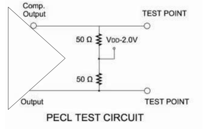
Each output is terminated with a 50 ? resistor to a termination voltage of (Vdd – 2V).
每个输出端接50Ω电阻,端接电压为(Vdd - 2V)。
What is LVDS Output?
什么是LVDS输出?
• LVDS stands for Low Voltage Differential Signaling,centered around operating voltage of 1.2V,regardless of power supply.
•LVDS代表低压差分信号,以1.2V的工作电压为中心,与电源无关。
• LVDS technology is defined by the ANSI/TIA/EIA-644 industry standard.
•LVDS技术由ANSI / TIA / EIA-644行业标准定义。
• Taitien has many crystal oscillator product lines with LVDS output options at 3.3V and 2.5V supplies.
•Taitien拥有许多晶体振荡器产品系列,具有3.3V和2.5V电源的LVDS输出选项。
Pros/Cons of LVDS Output
LVDS输出的优点/缺点
• Advantages:
• 好处:
– Lower power consumption compared to PECL outputs due to smaller voltage swings (typically ~350mV)
- 由于较小的电压摆幅(通常约为350mV),与PECL输出相比功耗更低
– Less susceptible to noise
- 不易受噪音影响
– Lower EMI emissions compared to CMOS/TTL
- 与CMOS / TTL相比,EMI辐射更低
• Drawbacks:
• 缺点:
– Reduced jitter performance compared to PECL
- 与PECL相比,抖动性能降低
Where is LVDS used?
LVDS在哪里使用?
The LVDS standard was created to address applications in the data communications, telecommunications,server, peripheral and computer markets where high-speed data transfer is necessary.
LVDS标准旨在满足数据通信,电信,服务器,外围设备和计算机市场中需要高速数据传输的应用。
Recommended LVDS Termination Circuit
推荐的LVDS终端电路
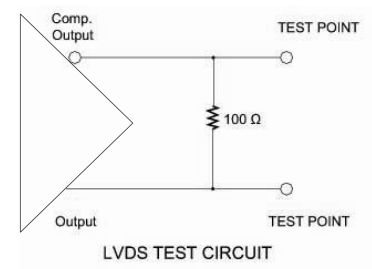
A single 100 ? termination resistor is needed. Some receiver ICs may include the resistor internally.
需要一个100Ω端接电阻。一些接收器IC可能在内部包含电阻器。
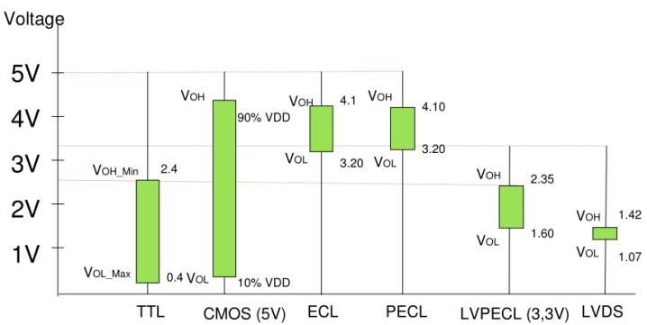
Signal Level Comparison
信号电平比较
什么是差分晶振的PECL和LVPECL?
• PECL stands for “Positive Emitter Coupled Logic”.PECL are differential logic outputs commonly used in high-speed clock distribution circuits. PECL requires a +5 V supply .
•PECL代表“正发射极耦合逻辑”.PECL是常用于高速时钟分配电路的差分逻辑输出。 PECL需要+5 V电源。
• Low Voltage PECL (LVPECL) denotes PECL circuits designed for use with 3.3V or 2.5V supply,the same supply voltage as for low voltage CMOS devices.
•低压PECL(LVPECL)表示设计用于3.3V或2.5V电源的PECL电路,电源电压与低压CMOS器件相同。
• Taitien offers LVPECL output crystal oscillators in both 3.3V and 2.5V supplies
泰艺晶振提供3.3V和2.5V电源的LVPECL输出晶体振荡器
Pros/Cons of PECL Output
PECL输出的优点/缺点
• Advantages :
• 好处 :
– Very good jitter performance due to large voltage swing
- 由于大电压摆动,具有非常好的抖动性能
– Ideal use in high-speed circuits
- 理想用于高速电路
– Capable of driving long transmission lines
- 能够驱动长传输线
• Drawbacks:
• 缺点:
– Larger power consumption due to differential output and external DC biasing compared to single-ended output
- 与单端输出相比,差分输出和外部直流偏置会产生更大的功耗
– Incompatible with 1.8V supply
- 与1.8V电源不兼容
Recommended PECL Termination Circuit
推荐的PECL终端电路
Each output is terminated with a 50 ? resistor to a termination voltage of (Vdd – 2V).
每个输出端接50Ω电阻,端接电压为(Vdd - 2V)。
What is LVDS Output?
什么是LVDS输出?
• LVDS stands for Low Voltage Differential Signaling,centered around operating voltage of 1.2V,regardless of power supply.
•LVDS代表低压差分信号,以1.2V的工作电压为中心,与电源无关。
• LVDS technology is defined by the ANSI/TIA/EIA-644 industry standard.
•LVDS技术由ANSI / TIA / EIA-644行业标准定义。
• Taitien has many crystal oscillator product lines with LVDS output options at 3.3V and 2.5V supplies.
•Taitien拥有许多晶体振荡器产品系列,具有3.3V和2.5V电源的LVDS输出选项。
Pros/Cons of LVDS Output
LVDS输出的优点/缺点
• Advantages:
• 好处:
– Lower power consumption compared to PECL outputs due to smaller voltage swings (typically ~350mV)
- 由于较小的电压摆幅(通常约为350mV),与PECL输出相比功耗更低
– Less susceptible to noise
- 不易受噪音影响
– Lower EMI emissions compared to CMOS/TTL
- 与CMOS / TTL相比,EMI辐射更低
• Drawbacks:
• 缺点:
– Reduced jitter performance compared to PECL
- 与PECL相比,抖动性能降低
Where is LVDS used?
LVDS在哪里使用?
The LVDS standard was created to address applications in the data communications, telecommunications,server, peripheral and computer markets where high-speed data transfer is necessary.
LVDS标准旨在满足数据通信,电信,服务器,外围设备和计算机市场中需要高速数据传输的应用。
Recommended LVDS Termination Circuit
推荐的LVDS终端电路
A single 100 ? termination resistor is needed. Some receiver ICs may include the resistor internally.
需要一个100Ω端接电阻。一些接收器IC可能在内部包含电阻器。
Signal Level Comparison
信号电平比较
正在载入评论数据...
相关资讯
- [2023-07-12]康纳温菲尔德推出符合Stratum3E...
- [2023-06-26]选择石英晶体要了解的必要参数,...
- [2023-06-25]艾伯康公司发布连续电压有源晶振...
- [2021-01-18]今日主题:什么样性能的石英晶振...
- [2021-01-13]是什么原因造成晶振相噪恶化?都...
- [2020-12-09]干货干货!爱普生旗下SG-8018系列...
- [2020-09-08]石英Crystal工作原理是怎样的,这...
- [2020-09-01]Oscillator的制造流程究竟是怎样...